
The continuous evolution of semiconductor materials has been a key enabler of progress in electronics and power conversion systems. For more than half a century, silicon has been the foundation of the semiconductor industry, delivering extraordinary performance improvements through scaling, integration, and cost reduction. However, as applications demand higher efficiency, higher voltage operation, and greater thermal robustness, silicon has reached fundamental physical and performance limitations.
The Rise and Limits of Wide Band Gap Semiconductors
In response, wide band gap (WBG) materials such as silicon carbide (SiC) and gallium nitride (GaN) have emerged and are now in commercial use across a wide range of applications. Their larger bandgaps, higher breakdown fields, and superior switching characteristics compared to silicon have enabled new levels of efficiency and power density in systems ranging from electric vehicles to renewable energy inverters and high-frequency power supplies. Nevertheless, even these materials face limitations in terms of thermal conductivity, defect density, and long-term reliability under extreme conditions.
Why Diamond is the Ultimate Semiconductor Candidate
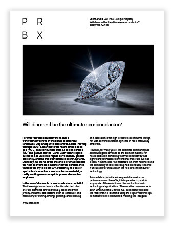
Against this background, diamond has been identified as a semiconductor material with properties that significantly surpass both conventional silicon and established WBG semiconductors. On paper, diamond possesses all the attributes required to become the ultimate semiconductor platform for next-generation power and high-frequency devices.
Research progress over the past decade has validated many of these theoretical advantages. Advances in synthetic diamond fabrication, particularly chemical vapor deposition (CVD), have enabled the production of high-purity, single-crystal substrates suitable for device development. Laboratory prototypes have demonstrated Schottky barrier diodes, field-effect transistors, and vertical devices capable of blocking kilovolt-class voltages.
| Material Property | Silicon (Si) | Silicon Carbide (4H-SiC) | Gallium Nitride (GaN) | Diamond (C) |
|---|---|---|---|---|
| Band gap (eV) | 1.11 | 3.26 | 3.39 | 5.47 |
| Breakdown field Ec (MV/cm) | 0.3 | 3.5 | 3.4 | 10.0 |
| Electron mobility μe (cm²/Vs) | 1,500 | 800 | 900 | 2,200 |
| Thermal conductivity (W/mK) | 150 | 490 | 200 | 2,130 |
Furthermore, hybrid approaches—such as GaN-on-diamond heterostructures and diamond heat spreaders—have already found early commercial use in radio-frequency (RF) devices, high-power laser diodes, and thermal management solutions for advanced processors. These hybrid applications highlight the potential of diamond to deliver tangible benefits even before the full commercialization of diamond-based semiconductor devices.
Critical Challenges to Diamond Semiconductor Commercialization
Despite this progress, significant challenges remain before diamond can become a mainstream semiconductor material. Doping diamond, particularly for stable n-type conductivity, remains a critical bottleneck. The availability and scalability of defect-free single-crystal diamond substrates are still limited, and fabrication processes require adaptation to diamond’s exceptional hardness and chemical stability. In addition, integration with existing packaging technologies and compatibility with conventional control and driver circuits must be addressed to enable system-level adoption.
Nevertheless, the promise of diamond is too significant to ignore.
Our latest White Paper introduces the potential of diamond as a semiconductor material, positioning it within the broader context of silicon and WBG semiconductors. By comparing diamond directly with established technologies, this study aims to highlight both the opportunities and the practical challenges associated with adopting diamond in electronic devices. While still in the research and development stage, diamond has the potential to redefine the boundaries of semiconductor performance, marking a new frontier in the ongoing evolution of materials for power and high-frequency electronics.
Download and read more in PRBX White paper 046:
Will diamond be the ultimate semiconductor?
WP 046 – 2025.10.06
Diamond is showing potential to outperform both silicon and wide band gap semiconductors in power electronics. This white paper explores its advantages in efficiency, voltage handling, and thermal performance – as well as the challenges ahead.
Learn more about it in our White Paper:
Will diamond be the ultimate semiconductor?
